Innatera is a semiconductor company that develops ultra-low-power neuromorphic processors for AI at the sensor edge. Its key product is the Spiking Neural Processor (SNP), which utilizes a revolutionary analog-mixed signal computing architecture to deliver brain-inspired cognition performance within an extremely low-power envelope. The SNP combines a Spiking Neural Network engine and a RISC-V processor core.
At CES 2025 in Las Vegas, JPR’s David Harold met with Innatera CEO Sumeet Kumar and CMO Shreyas Derashri to learn about a Spiking Neural Processor (SNP) and its usefulness in edge AI applications. Innatera claims its SNP can process sensor data with 500X less energy and 100X faster compared to conventional approaches. If so, this would be a dramatic improvement in efficiency and speed that could enable always-on, real-time AI capabilities in battery-powered and edge devices that were previously not feasible.

What is Innatera all about? Where does it come from, and why should it exist?
Kumar: So, we’re a semiconductor company that spun out of Delft University of Technology in 2018. Our mission is to bring brain-like intelligence to sensors everywhere. The key problem we’re addressing is that sensors produce massive amounts of data, but the AI value chain has grown inefficient. We saw an opportunity to process much of the world’s sensor data directly at the source.
Our company started with about 10 years of research into brain-inspired and energy-efficient computing. Since then, we’ve grown to over 80 employees spread across 15 countries and have raised €25 million (about US$25.7 million) in funding from leading European deep-tech investors.
When we began in 2018, we identified a huge opportunity: Sensors are everywhere—4 billion new devices are produced each year, all packed with sensors. Many of these sensors are used in applications involving human-machine interaction or automated operations. We envision creating an ‘ambient intelligence,’ where living spaces respond intuitively and seamlessly to your intent without explicit commands. This enhances digitization and improves quality of life.
The problem is that today’s sensors generate large amounts of data, which often has to be processed in the cloud. This approach consumes a lot of energy, introduces latency, and increases costs. The solution is to move intelligence closer to the sensor, but most devices are battery-powered, and the limited energy available restricts the level of processing that can be done. This is the challenge we’re addressing with our Spiking Neural Processor.
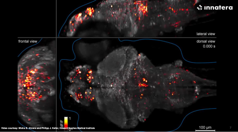
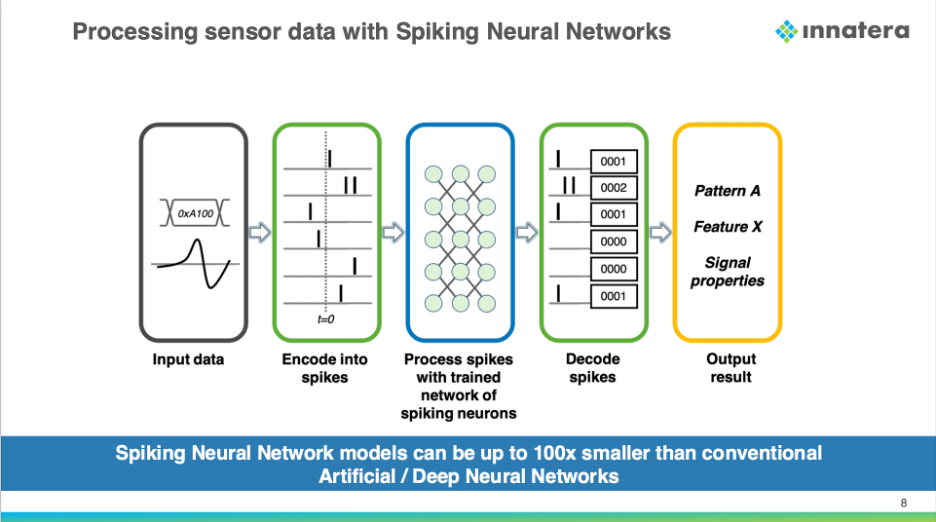
Our processor mimics how the brain recognizes patterns in sensory data. For example, when you see, hear, or smell something, your brain identifies patterns using clusters of neurons. We’ve translated this principle into a technology called spiking neural networks, which inherently understand time and enable AI functionality using neural networks that are 100 times smaller than those in use today.

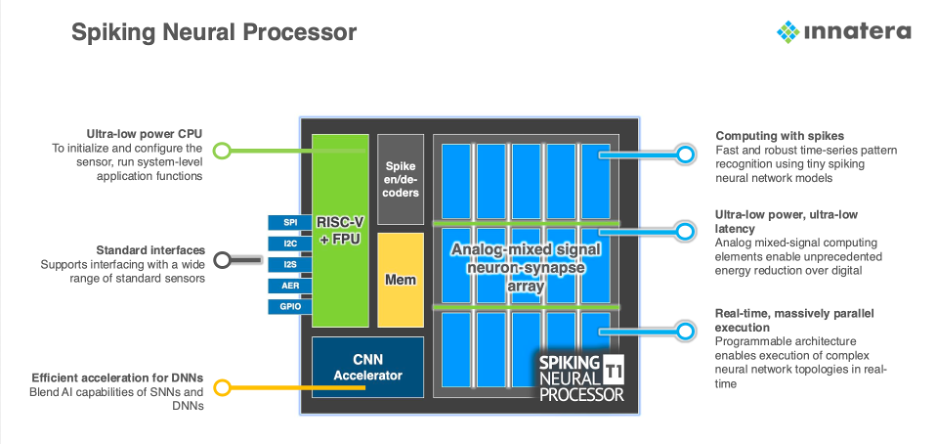
We’ve developed chips specialized for running spiking neural networks. Our architecture, called the Spiking Neural Processor, is designed for massively parallel processing with very low latency and minimal power consumption—less than a milliwatt in most cases. The T1, which we announced at CES last year, is the world’s first neuromorphic microcontroller that delivers ultra-low-power AI directly at the sensor. It combines our spiking neural network acceleration with conventional AI acceleration and a RISC-V CPU to provide application designers with a single-chip solution for efficient AI capabilities.

How are these chips used in different applications?
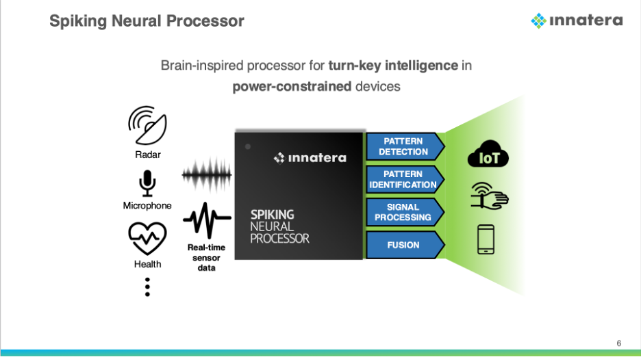
Kumar: In simple devices like door-opening systems, smart lighting, or smoke detectors, our chip is often the only processor in the system. It converts raw sensor data into actionable insights with very low power consumption. In more complex devices, such as video doorbells with an existing applications processor, our chip acts as the sensor-handling engine. It off-loads all sensor data processing from the applications processor, making the system much more efficient by waking up the more power-hungry system only when there is some actionable information from the sensor.

Does the applications processor treat your chip as part of a heterogeneous system, controlling it, or does your chip operate independently?
Derashri: For most applications, the apps processor treats us like an extended sensor. We work independently and don’t require control from the apps processor. Our chip includes its own RISC-V CPU and can function autonomously.
Kumar: The chips are programmed using a powerful software development kit (SDK) we call Talamo. It uses PyTorch as the front end for model development, allowing developers to build neural networks for our chips using standard Python tools. Once the model is trained and optimized, the SDK maps it onto the chip, so developers don’t need to understand the chip’s internals. The SDK also includes extensive libraries for standard applications and modular components, making it easy to piece together models, like building with Lego blocks. This simplifies AI solution development for sensing applications and reduces time to market.
How does your chip compare to competitors’ in terms of performance?
Kumar: Across benchmarks, we’ve achieved radical energy and latency reductions, while maintaining or exceeding the accuracy of competitors. For instance, in audio applications, we see energy reductions of 80–100X compared to leading solutions, with comparable accuracy. In radar applications, our chips achieve a 42X power reduction and a 170X latency reduction, all while consuming less than a milliwatt of power.

What accuracy levels do you support, and can you adjust accuracy based on requirements?
Kumar: For tasks like audio scene classification, we use the DCASE2020 benchmark dataset. The state-of-the-art accuracy is around 90%, and our solutions achieve greater than 91% accuracy with less than a milliwatt of power consumption. Many competitors report lower power numbers but sacrifice accuracy. For example, they might achieve 50% accuracy at 150µW, but to reach 90% accuracy, their power consumption rises to 20mW. We maintain high accuracy while keeping power consumption extremely low.
Are you targeting specific markets with these chips?
Kumar: Our primary focus is the consumer electronics market. However, we also have significant opportunities in areas like IoT, smart homes, and industrial predictive maintenance. For instance, in radar applications, we offer highly differentiated solutions for IoT and smart building markets.
Do you also license your technology as IP, or are you focused solely on selling chips?
Derashri: While there is interest in licensing our technology as IP, it’s a challenging path because the technology is complex. For now, we’re focused on selling chips and chiplets.
What about security? How do you ensure data protection?
Derashri: Our chips are standard microcontrollers with built-in security features. For now, we’re focused on bare-metal implementations. If needed, we can isolate protected areas, but we haven’t seen a requirement for something more complex like cryptographic solutions yet.
Kumar: As a company, we’ve been developing this technology for years. We entered production last month with our seventh-generation chip, the production version of the T1. We’ve been sampling the T1 to customers since 2024, and our development kit allows customers to experiment with different applications. For example, our chip enables robust human presence sensing in devices like doorbells or smoke detectors, significantly extending battery life compared to traditional designs.
What’s next for Innatera?
Kumar: We’re scaling up production volumes and expanding our customer base. Our chips are already being used in innovative applications, and we’re excited to see how they’ll continue to transform sensing technology.
LIKE WHAT YOU’RE READING? INTRODUCE US TO YOUR FRIENDS AND COLLEAGUES.